

For some years now it has been clear that we have moved into a new “Cold War”, which is both similar to and significantly different from the previous one. We have mentioned many times (bordering on platitude, but it is extremely important to realize its importance) that we live in the Age of Information. This 4th industrial revolution was made possible by a series of discoveries and innovations, which we can safely say are related to communication and information systems technologies. The internet, which started in the 60s as ARPANET, has seen the number of interconnected devices from a few dozen in the 70s, to hundreds of billions in 2020, and the number continues to grow. Now, the Internet of Things (or Internet of Things) as well as the future Internet of Everything, are driving but also testing the technological – and not only – limits.
This explosive growth is essentially based on our ability to manufacture increasingly advanced chips. The word chips is misused here, as it describes a huge family of devices, which include integrated circuits such as mainframe computers, micro-controllers, or memory circuits. The basis of all this is the transistor, and the industry’s ability to integrate an ever-increasing number of transistors within the surface of a chip is the driver of these developments. The famous Moore’s law (Moore’s law) describes this very possibility, and predicts that the number of transistors observed on the surface of a chip will double approximately every two years.
The entire technology is based on semiconductors, which are materials whose specific resistance value varies between that of insulators and that of conductors. It is observed that it rapidly decreases with increasing temperature (a reason why cooling plays a huge role in the performance of modern computing systems). Semiconductors can be elements, such as silicon (not to be confused with silicon!) and germanium, or chemical compounds, such as gallium arsenide or cadmium selenide. Both gallium and cadmium are rare elements, which is not the case with silicon, which is the second most abundant chemical element after oxygen. In fact, silicon reacts easily with oxygen, giving various silicate compounds (mainly silicon dioxide).

Because silica reacts easily it is usually found in the form of quartz or silica sand. With a method – known as the Czochralski method – we take bars of pure (99%) silicon, which we cut into slices, known as wafers (yes, it means wafer!). After being cleaned and polished, they are coated with special – photosensitive – chemicals and are ready for further processing. So far the process is neither difficult nor complicated and a Czochralski furnace can also be purchased from the internet, costing a few tens of dollars. The next stage is what differentiates both quality and performance.
“Imprinting” the circuit design on the wafer is based on a complex process called photolithography. The most complex and specialized form in industrial application at the moment is called Extreme Ultraviolet Lithography (EUV), and it allows scales down to 5 nm (nm = nanometers). To understand the relative sizes, a red blood cell is 7000 nm in size while a virus is 14 nm. The wavelengths are so short (13.5 nm) that the entire process must be performed in a vacuum! Currently, this technology allows Apple’s M1 Ultra chip to have 114 billion transistors on its surface! There are very few companies that can manufacture such chips, with the one with the largest production on the planet being TSMC (based in Taiwan), which supplies Apple, NVidia, AMD, etc.
Lately, China has threatened to invade Taiwan in order to bring it back into the metropolitan core. Many – perhaps mockingly – estimate that access to TSMC alone is enough for China to cross its Rubicon, the Taiwan Strait. But TSMC, although it is the largest producer, is ABSOLUTELY dependent in turn on another company, which holds the ABSOLUTE MONOPOLY in the manufacture of the machines, which take advantage of the EUV technique. Such a machine requires huge investment in both human and financial terms, takes months to build and months to transport, and is the size of a bus. It incorporates the top of the relevant technology and costs at least $150 million each!

This company is none other than ASML Holding N.V (also known as Advanced Semiconductor Materials Lithography) and is based in Veldhoven, the Netherlands. It is the most valuable European technology company, in terms of capitalization, which amounts to 200 billion euros! It is also preparing a new device, which will be based on the EUV High Numerical Aperture technology – which allows lithography at 2 nm – and which will cost more than $350 million. It is no coincidence, then, that the US and the EU are cooperating closely in support and entrenching their leadership in the specific field.
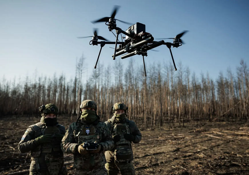
China currently cannot go below 7nm, which is also the absolute limit of DUV technology. Other countries, such as Russia (even before sanctions) will have to find various imaginative and unimaginative ways to gain access to the chips. It is indicative that chips from European and American companies were found in Russian drones and UAVs, without being able to clarify how they got there. The recent US enactment of the CHIPS and Science Act, which – among other things – provides $280 billion for the further development of domestic technologies as well as closer cooperation between the US and the EU, is moving in the direction of a war for supremacy in technological field.
We should not forget that China has access to most of the world’s rare earth deposits, and any access to EUV technology would put it at a huge advantage over all other countries. It is no coincidence that ASML spends (apparently) €60 million every year to prevent industrial espionage-related attacks. After all, the heart of modern technology does not beat on an island, thousands of kilometers away, but within our European neighborhood. The question is, how ready are we as the West to preserve and enhance this technological advantage, and for how long.
